Musk Calls IBM's '0.7nm Chip' Label Misleading, Proposes Naming by Atom Count
Semiconductor process node names stopped being literal a long time ago. The number that used to refer to the gate length of a transistor — 7nm, 5nm, 3nm — now functions more as a generational marketing label than a measurement. But Elon Musk thinks the industry has taken that abstraction a step too far.
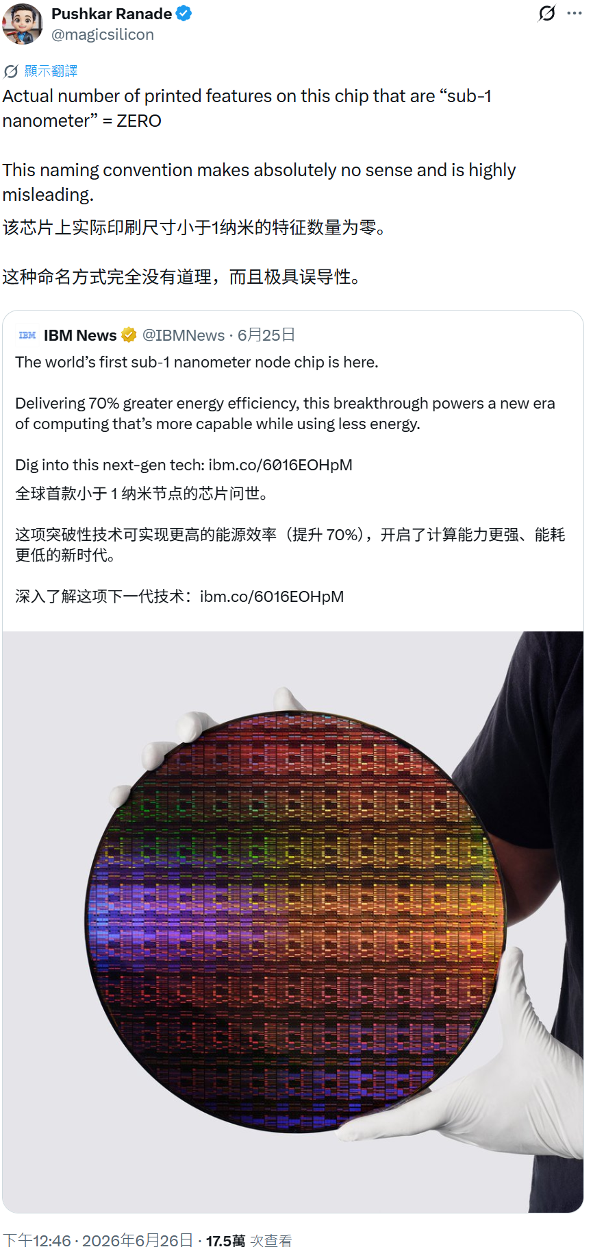
The billionaire weighed in after a post on X pointed out that IBM’s newly announced “0.7nm” chip — which the company also calls 7Å (angstrom) — contains zero printed features smaller than 1 nanometer. The post called the naming “completely nonsensical and extremely misleading.” Musk agreed, and went further.
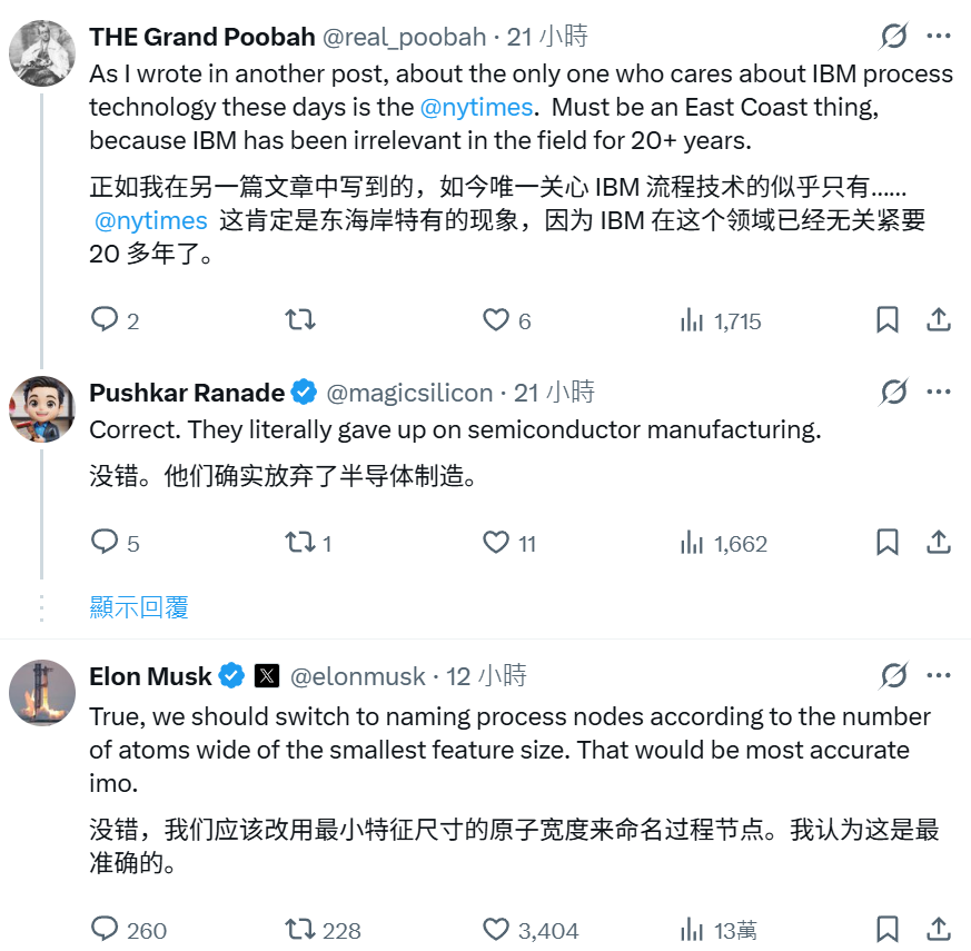
“We should name process nodes by the number of atoms corresponding to the minimum feature width,” Musk wrote on X. “In my opinion, that would be the most accurate way to name them.”
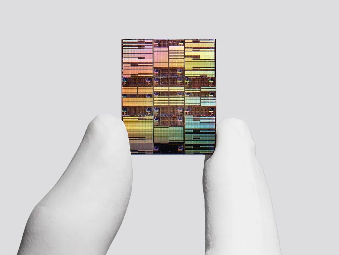
IBM unveiled its 0.7nm (7Å) process earlier this week, describing it as an evolution of its Nanosheet transistor technology. The company’s new Nanostack approach stacks transistors vertically to boost density, and wafer bonding plays a key role in the process. IBM positioned the announcement as a look ahead at next-generation chip fabrication.
IBM directly addressed the naming controversy, defending its choice by pointing to industry precedent.
“Like the naming convention for transistor sizes in recent years, ‘7 angstrom (7Å)’ refers to chips manufactured using a specific fabrication process in this generation,” IBM explained. It acknowledged that “7Å” does not refer to the actual width of contact metal wires used in older chips — an era when integration densities were far lower.
Musk’s response came after he encountered a post on X arguing that IBM’s naming made no sense. The post noted that IBM’s chip has zero features smaller than 1nm printed anywhere on it. Musk agreed, then proposed a different approach entirely.
“We should name process nodes by the number of atoms corresponding to the minimum feature width,” he wrote. “In my opinion, that would be the most accurate way to name them.”
The exchange highlights a growing tension in the semiconductor industry. As chip features approach atomic scales — a single silicon atom measures about 0.2nm across — the old nanometer-based naming system becomes increasingly detached from physical reality. Intel, TSMC, and Samsung have all abandoned their earlier naming conventions at various points, often switching from process node numbers based on transistor density to labels that reflect generational improvements.
Musk’s atom-count proposal would sidestep the confusion entirely. A 7Å minimum feature would correspond to roughly 3-4 silicon atoms across, depending on the crystal orientation. Under Musk’s system, the node might be called something like “4-atom” rather than “0.7nm” or “7Å.”
Whether the industry adopts Musk’s suggestion is another question. Semiconductor marketing has never been known for strict adherence to physics — what matters to chip buyers is performance, density, and power efficiency, not what the node number happens to be. But the debate itself underscores how far process node names have drifted from their original meaning.