Standing DRAM on Its Side Could Make AI Chips 82% Faster
AI accelerators have a heat problem. Stack DRAM layers higher to feed data to a GPU, and temperatures climb past 80°C. Push more bandwidth through the stack, and the thermal ceiling hits even faster. Two research teams have now proposed the same radical fix: stand the memory chips on their side.
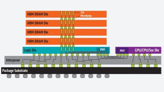
At the IEEE/JSAP Symposium on VLSI Technology in June, researchers from UNIST (Ulsan National Institute of Science and Technology) in South Korea and a separate team led by the University of Tokyo each presented architectures that rotate DRAM dies 90 degrees — from horizontal stacking to vertical placement. The shift eliminates the need for through-silicon vias (TSVs), the vertical interconnects that carry data through conventional HBM stacks, and opens up space for liquid cooling channels between dies.
The Korean team’s design, called V-Die, replaces TSVs with I/O connections along the bottom edge of each vertically standing die. With a connection pitch of just 20 microns, a V-Die stack can pack four times as many interconnects as HBM4. Memory read time drops 37% as a result.
In simulations matching H100-class hardware with a 16-layer stack, V-Die cut first-token latency by 32% — roughly 24 milliseconds. On GPT-3-scale workloads, the design pushed throughput to 540 tokens per second, compared to 296 tokens/s for a comparable HBM4 setup. That is an 82.43% improvement — not theoretical paper math, but from a validated simulation against real hardware parameters.
Heat is where V-Die separates itself most sharply from conventional HBM. The vertical arrangement allows microfluidic coolant to flow between dies, keeping the stack temperature around 45°C. High-density HBM systems routinely run above 80°C, which forces downclocking and caps sustained performance.
The Tokyo-led MOSAIC team took a different approach to the same vertical-stacking idea. Their design uses orthogonal die stacking with contactless interconnects — tiny inductive coils that replace physical metal contacts. The prototype interface runs at 4 Gbps per channel, and in a DRAM-on-GPU configuration, MOSAIC can deliver twice the capacity of HBM4 without the same thermal penalty.
A related variant, bump-MOSAIC, was demonstrated at the ECTC conference. It uses 100-micron-pitch micro-bumps with alignment error held under 6 microns (verified by X-ray CT). The team reports that this configuration achieves three times the thermal conductivity of conventional stacked HBM, with room for up to 30% more memory capacity per stack.
Neither V-Die nor MOSAIC is production-ready. Both are research prototypes that face significant manufacturing hurdles — vertical die handling is not something existing HBM fabs are set up to do at scale. But the direction is clear: the next bottleneck for AI hardware is not compute, but getting data in and out of memory fast enough without melting the package.