SanDisk's New Patent Stacks NAND Flash Beneath Compute Chips to Crack the Storage Bottleneck

There is a quiet tension running through every AI datacenter on the planet right now: the compute is getting faster, but the storage delivering data to those hungry accelerators is struggling to keep pace. Memory bandwidth, capacity, and — increasingly — physical proximity to the silicon have become the real ceilings on what a training run or inference workload can achieve.
IT-NEWS, June 22 — SanDisk is exploring a more radical way out. Rather than tweaking the DRAM roadmap or adding yet another tier of cache, the company has published a patent that proposes stacking NAND flash directly underneath the main compute die — be it a GPU or a dedicated AI accelerator — creating a tightly integrated compute-and-storage package that shares a single interposer with conventional HBM stacks. It is an architecture that, on paper, promises to collapse the distance between massive-capacity storage and the logic that needs it, while keeping low-latency DRAM right where it belongs for high-priority workloads.
The pressure behind the idea is real. The artificial intelligence boom has exposed performance bottlenecks that were once manageable. For years, the industry’s answer to growing memory demand was straightforward: ship a denser, faster DRAM generation and move on. But with fabrication costs climbing, yields under strain, and power envelopes blowing out, that playbook no longer works on its own. High-bandwidth memory — the stacked DRAM that sits alongside today’s leading AI chips — has become a bottleneck in its own right, constrained by limited manufacturing capacity and per-stack capacities that top out at a modest 32 to 64 GB.
There is a deeper physical problem, too. HBM stacks, by design, live off to the side of the main chip. Data travelling between them traverses the interposer and encounters latency that, while acceptable for many workloads, adds up quickly at scale. And HBM is not cheap. NAND flash, by contrast, offers vastly more gigabytes per dollar and much higher per-device capacities, but its penalty is distance: sitting further from the compute die, it cannot match the read and write bandwidth of DRAM-class memory. The industry has long treated this as an either-or trade-off. SanDisk’s patent — US 12,430,274 B2 — argues you can have both.
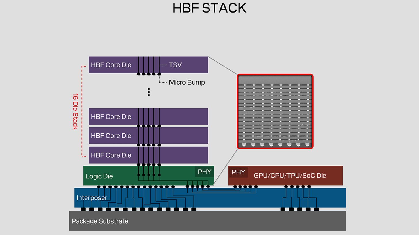
The core of the idea builds on High Bandwidth Flash, or HBF, a concept SanDisk has previously discussed. HBF borrows from the HBM playbook, stacking multiple NAND flash layers vertically and connecting them with thousands of through-silicon vias, creating a single integrated flash stack. Where one HBM stack might deliver 32 to 64 GB, a single HBF stack can scale to 4 TB. That alone addresses capacity. But the new patent takes a decisive step further.
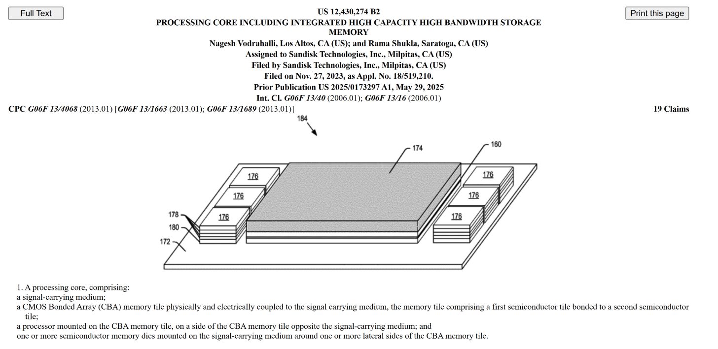
Instead of keeping the flash stack off to the side, the architecture places a NAND storage die — bonded with a CMOS Bonding Array layer — directly beneath the main compute die. The processor, be it a GPU or AI accelerator, sits on top; the NAND with its logic layer sits beneath; and the entire assembly is fixed onto an interposer that also carries HBM DRAM stacks along one or more edges. Each memory type takes on a distinct role. HBM handles the low-latency, high-priority reads and writes that the processor needs instantly. The under-chip NAND handles the bulk — large-capacity, high-throughput data operations where latency is less critical but volume is enormous. A wide-channel interconnect between the NAND die and the compute die keeps latency, hardware cost, and overall power consumption lower than what you would get from a traditional side-mounted bulk storage solution.
What SanDisk has laid out is not a product roadmap so much as a patent fortress. The detailed interposer wiring schemes, the CMOS bonding approach, and the die-to-die interconnect topology described in the filing would be difficult for competitors to replicate without running straight into the company’s intellectual property. At the same time, this remains a patent — not silicon you can buy. Bringing such an architecture to production means solving for total package power, managing the thermal overlap between NAND and logic, and taming the manufacturing cost of co-packaging two fundamentally different memory technologies in a single package.
The gap between what the patent envisions and what the market ships today remains wide. Current commercial products are coalescing around simpler side-by-side configurations that are already proven and cheaper to build. The question worth watching is whether SanDisk can bridge the distance between this patent-protected frontier architecture and the volume products it sells. The public technology announcements are the surface news. This patent is the deeper strategic blueprint.