Huawei's Chip Chief Publishes Updated 'Tao's Law' With Kirin 2026 Production Data
Huawei’s semiconductor chief He Tingbo dropped the second version of what the industry calls “Tao’s Law” on Wednesday — and unlike most academic theory papers, this one comes with real production measurements from the Kirin 2026 line.
The paper, posted July 3 on ChinaXiv (the Chinese Academy of Sciences’ preprint platform), is formally titled “A Time Scaling Theory for Multi-Layer Electronic Systems.” The V1 version from May 25 laid out the theoretical framework. V2 fills in the engineering details: actual measured data, physical implementation schematics, and a concrete product roadmap.
The central argument is that Moore’s Law-style scaling isn’t dead — it’s just moved into the third dimension. The theory uses a time constant τ as the fundamental scaling parameter for post-Moore semiconductor design. Instead of shrinking transistors on a flat plane, you stack logic vertically.
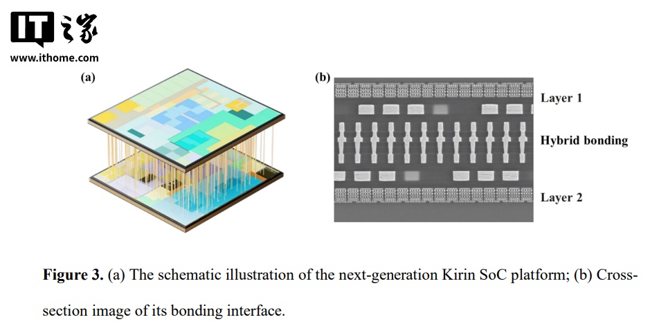
What makes V2 different is how much deeper it goes. The paper now runs eight chapters with a cleaner logical flow. He Tingbo added principle diagrams and physical images covering the τ-layered spacetime model, the LogicFolding architecture, bonding interface cross-sections, the Unified Bus interconnect, and the Hi-ONE optical engine.
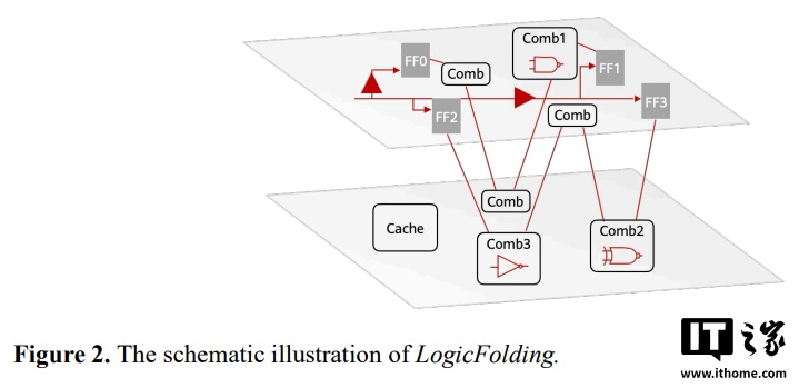
The headline technology is LogicFolding. V2 introduces the concept of a “gear ratio” — when the hybrid bonding pitch approaches the top metal layer wiring dimensions, the 3D design space shifts from traditional “macro-block level discrete optimization” to “unit-level continuous optimization.” In plain English: instead of stacking whole functional blocks on top of each other like pancakes, you can now fold logic at the individual cell level. That’s a genuine advance in how 3D chips are designed.
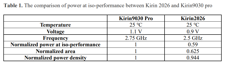
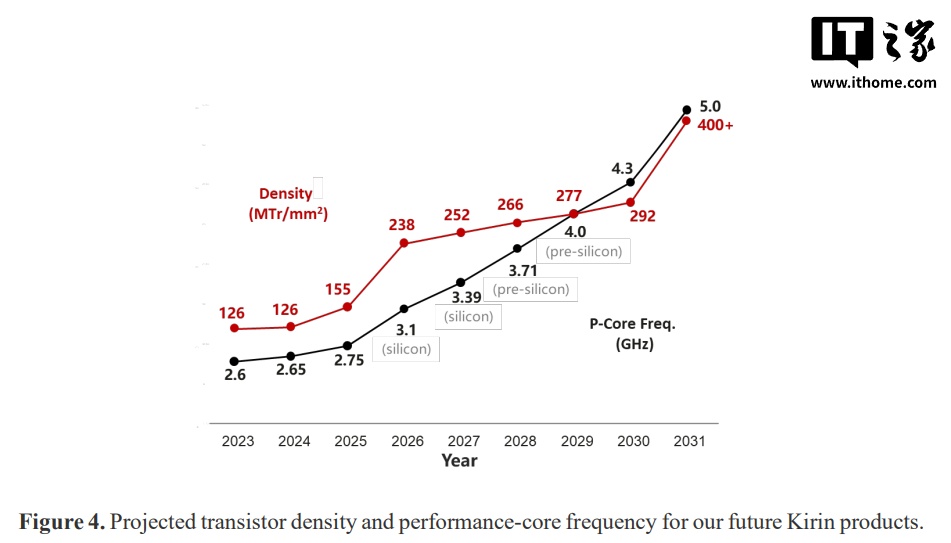
The production data is what separates this from a theoretical exercise. V2 includes a measured data table comparing the Kirin 2026 against the baseline Kirin 9030 Pro — voltage, frequency, normalized power consumption, area, and power density figures from actual wafers. These aren’t simulated projections.
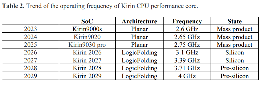
The paper also lays out a technology roadmap. On the mobile side, it tracks TSV (through-silicon via) migration from the top metal layer down to the M6 layer, plus multi-active-layer stacking. On the AI side, it specifies the iteration cadence for the Ascend accelerator series.
Tao’s Law is named after the Chinese phonetic reading of the paper’s central character τ (tau). Whether it gains traction as a named law in the semiconductor industry the way Dennard scaling or Moore’s Law did remains to be seen — but the inclusion of real Kirin 2026 data suggests Huawei is serious about treating this as more than an academic publication. The full paper is available on ChinaXiv for those who want the equations.